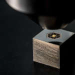
Verifying a mould’s dimensions for a RF tag printed by inkjet
The Barcelona Microelectronics Institute (IMB) is the National Microelectronics Centre (CNM)’s Barcelona location and a member of the Spanish Research Council. IMB-CNM has a focus on basic and applied research and development, in addition to education and training in micro and nanotechnologies, components and systems. Our mission is to expand the knowledge available in this field and to contribute to the implementation of solutions and new products based in these technologies in order to resolve the challenges faced by society today.
With Sensofar’s 3D optical profiler we are able to check the mould height and calculate if there will be a sufficient layer of silver bulk to achieve the desired conductivity for good performance
When using functional inks with inkjet technologies to create microelectronic devices, there’s a need to verify any differences between the desired design and what’s actually printed; the height and shape of the printed layers is integral to optimal device configuration and functionality. Verifying mould’s dimensions we ensure it.
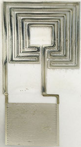
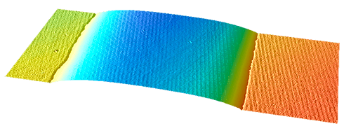
The antenna’s mould has 4 tracks that create 5 valleys that are filled with silver ink. Each mould track is 600 µm wide and 15 µm high.
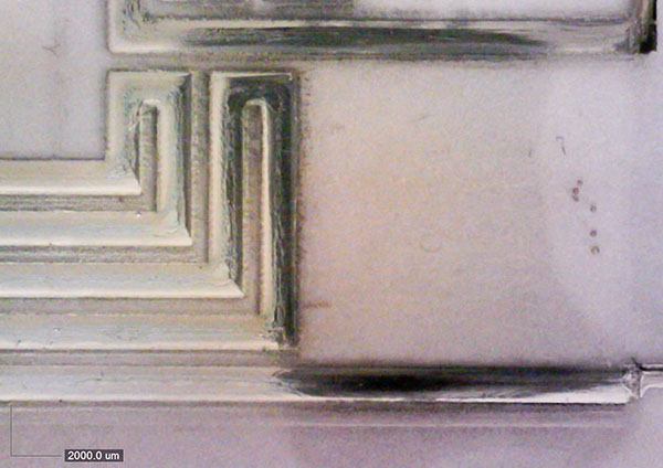
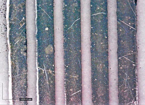
The device’s purpose is measuring e-coli bacteria on a hand-paper dispenser where the tag is printed on the paper. The antenna is connected to an interdigitated capacitor that behaves like a bacterial sensor, when there are changes the capacitor’s value affects the antenna resonance’s frequency; these variables are easy to measure with a RF transceiver.
Currently, these kinds of devices tend to use contact profilometers that provide measures that aren’t as precise as we need them to be.
With Sensofar’s 3D optical profiler we are able to check the mould height and calculate if there will be a sufficient layer of silver bulk to achieve the desired conductivity for good performance.
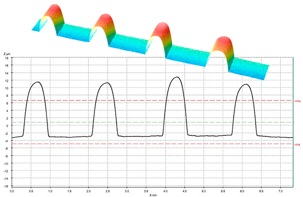
By verifying with a Sensofar Plμ neox using the confocal technique with a 20X brightfield objective that the RF antenna’s shape was as desired and possessed an adequate silver layer, good conductivity was ensured.
The Sensofar equipment provided non-contact 3D surface profilers based on three technologies: Confocal, Interferometry and Focus Variation techniques and allowed us to obtain high-resolution measurements in a fast and non-destructive way, with user-friendly software for technical support.
