Improving the measurement of thick and thin films with optical profiling techniques
Partner at Sensofar since 2004.
Experienced Research & Development Specialist, Cristina works at CD6 as R&D Engineer since 1996 and she is Software Manager at Sensofar Tech SL since it’s foundation in 2001 and VP Software since 2017. The research interests include optical metrology, surface metrology, image processing and computing sciences. Since 2010 she is developing the use of three-dimensional (3D) topographical analysis in firearms analysis.
Improving the measurement of thick and thin films with optical profiling techniques full article
Cristina Cadevall1, C. Oriach-Font1, Roger Artigas1, Agustí Pintó1, Ferran Laguarta1
1Universitat Politècnica de Catalunya (UPC) Rambla Sant Nebridi, 10, E-08222 Terrassa, Spain.
Proceedings Volume 6616, Optical Measurement Systems for Industrial Inspection V; 66161Z (2007)
Event: Optical Metrology, 2007, Munich, Germany
Abstract
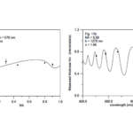
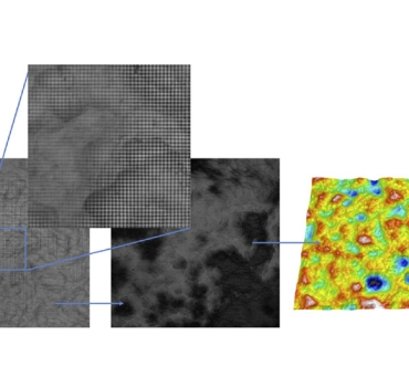
Optical profiling techniques, mainly confocal and white light interferometry, have demonstrated to be suitable techniques for characterization of transparent thick films. Measurements are carried out by vertically scanning the upper and lower film interfaces. Thickness of the layer is determined from the two peaks in the confocal axial response or from the two sets of interference fringes developed during the vertical scan. The 3D topographies of the upper and lower interfaces of the film can also be obtained. Measurements of photoresists or oxide coatings are typical examples of thick film characterization. On the other hand, measurement of thin films is considered to be a very difficult application to carry out with most optical imaging profilers. A film should be considered as thin when the two peaks obtained along the vertical scan become unresolved. We introduce new methods based on confocal techniques, which make it possible to measure sub-micrometric layers on structured samples. These techniques are based on the comparison between the axial responses obtained in areas where the film is present and those in other areas where only the substrate is present. This method has been successfully used for thickness assessment of several samples, such as a set of calibrated Si-SiO2 layers.


