APPLICATIONS
Semiconductors
< All applications
For semiconductor applications, Sensofar’s products can characterize critical dimensions, roughness, and perform defect inspection, frequently within the back-end packaging of the manufacturing process.
Silicon Carbide Wafer
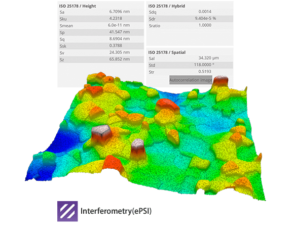
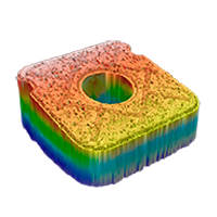
Silicon Carbide (Si-C) wafers have astonishing electrical and thermal properties making them a must for certain applications, like 5G chips. As CVD (Chemical Vapor Deposition)is used in their production, characterizing their surface finish helps to understand if the lattice growth will be homogeneous.
Height, hybrid and spatial parameters in SensoVIEW allow us to characterize the crystals well.
Etched circuit
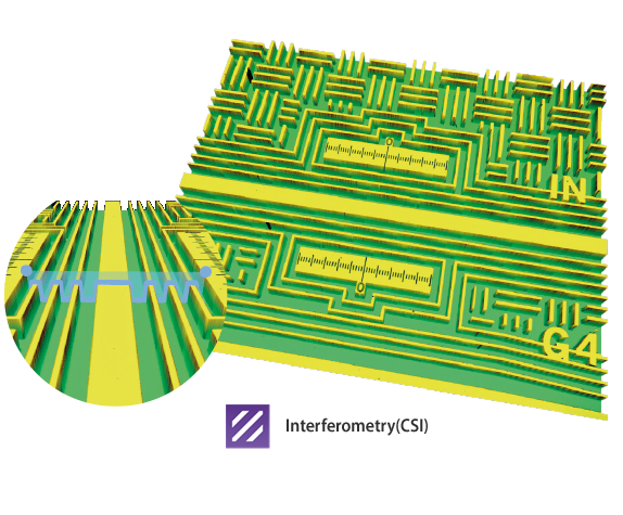
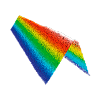
After an etching process, it is typical to evaluate the height of the resulting features. The Step Height SensoPRO plugin detects the two height levels, regardless of the analyzed pattern, will be immediately identified. To ensure the best accuracy on the measurement, interferometry is used.
3D Cross Kerf
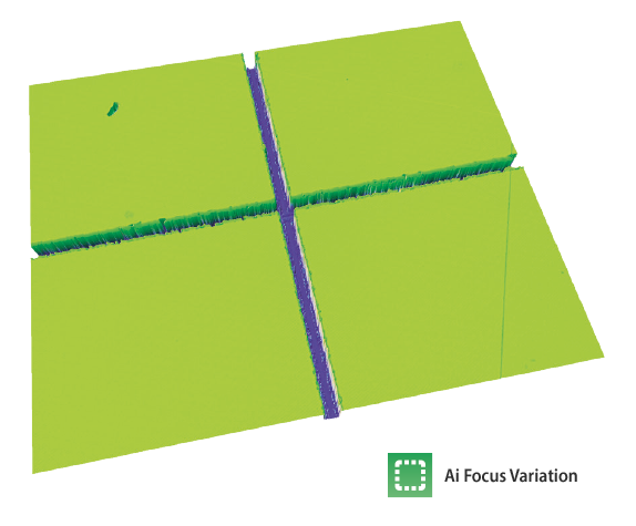
Chip segmentation has two main dimensions to characterize: height, to ensure that the bottom is not damaged, and width, which is a measure of the quality of the cut. Cross kerf plugin not only detects the cross and extracts the desired parameters but also levels the surface to make sure that an existing angle in the wafer doesn’t affect the extracted data. The high aspect ratio of those dimensions is challenging and only Ai Focus Variation can resolve this application.
Passivation
layer hole
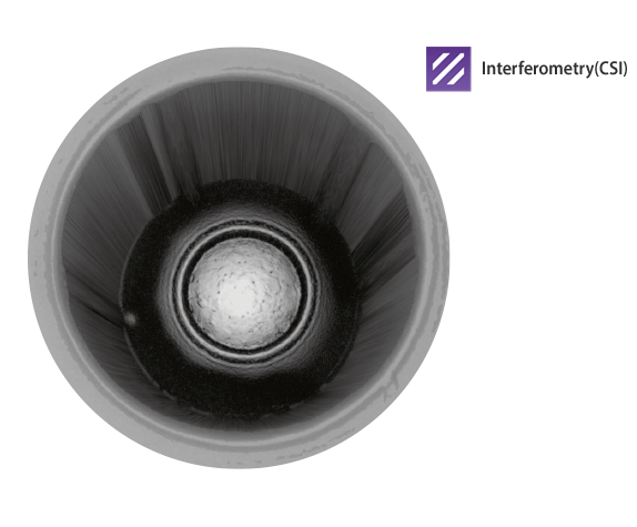
Passivation layer holes determine the access of wire bonding on a chip.
The Hole plugin is useful in this application since it can measure holes from 50 µm to 2 mm in diameter.
Thin film
inside holes
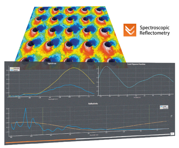
The S neox exceeds the applications for Spectroscopic Reflectometry since it can measure inside holes with very small diameters using a spot size down to 3 µm!
Wafer warping through structure measurement
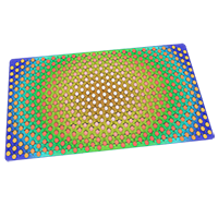
This wafer has been through different processes which explain its characterization: firstly, a texturizing process, making it quite rough and, consequently, measurable with the S wide.
Secondly, an epitaxy growth has been carried out and with it the wafer has been exposed to high temperatures, leading to potential wafer deformation. To assess that, we have measured the distances between its structures with SensoVIEW, to see if they match the expected lengths.


