APPLICATIONS
Integrated Circuit (IC) Packaging is the last stage of semiconductor manufacture and consists of the encapsulation of a semiconductor component. We mainly measure the dimensions of the pins and their surface finish so they connect properly to the PCB.
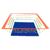
BGA package
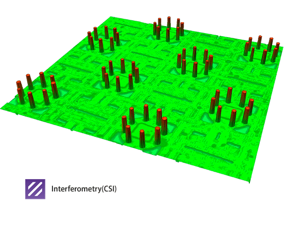
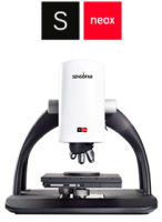
BGA (Ball Grid Array) packaging is a structure for Surface Mount packaging. The inspection is only completed after checking each ball to ensure a good connection with the PCB. Our S neox, used alongside SensoPRO provides a fast and fully automated solution to measure the height of each ball.
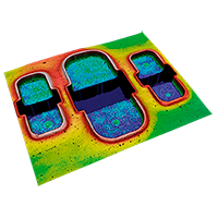
Thermal pad
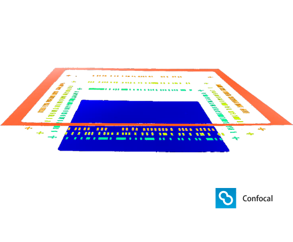
When there are parts that need to be characterized in multiple ways such as this thermal pad, SensoPRO has a solution: it can analyze the sample with different plugins simultaneously, getting a very comprehensive analysis.
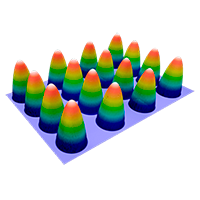
Wire bonding
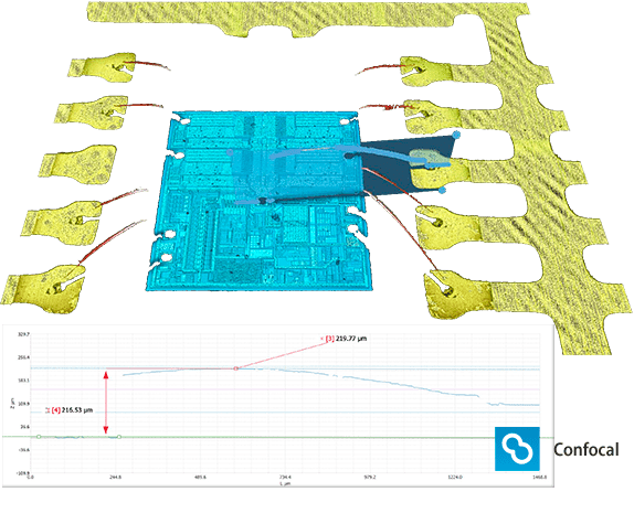
Technology always pushes limits. Sensofar wants to be at the forefront. Vanguard technologies reduced the diameter of gold wires down to 30 µm, a significant improvement.
SensoVIEW can create as many profiles as needed and measure critical dimensions. This example shows the height difference between the maximum point of the wire and the chip since that parameter will determine whether or not the cable makes contact with the chip’s cover.
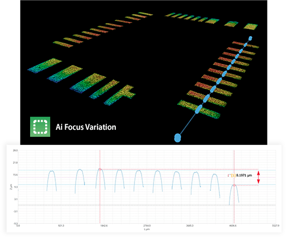
QFN Pins
One of the most popular IC packaging types is the QFN (Quad-flat No Lead) packages because they are suitable for many users in consumer, automotive, or power applications. The flatness of the pins is the evaluated element. Using the SensoVIEW profile tool we can evaluate the flatness of the pins.
QFN thermal pad
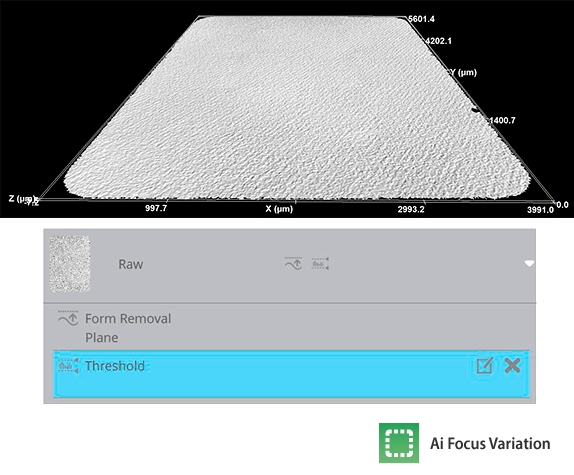
Flatness (Sz) is crucial to ensure a good attachment between a pad and the bottom of a chip to allow proper heat dissipation.
Flatness assessment is straightforward with SensoVIEW. To avoid possible spikes in the measurement, we apply leveling and thresholding and then we get the Sz value. SensoVIEW calculates roughness parameters on the dataset, by default. Then we need just to save this processing and apply it to the dataset.
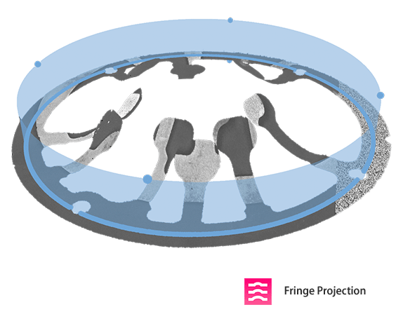
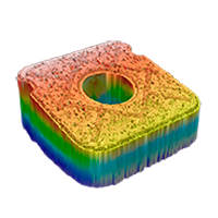
Cover of 5G component
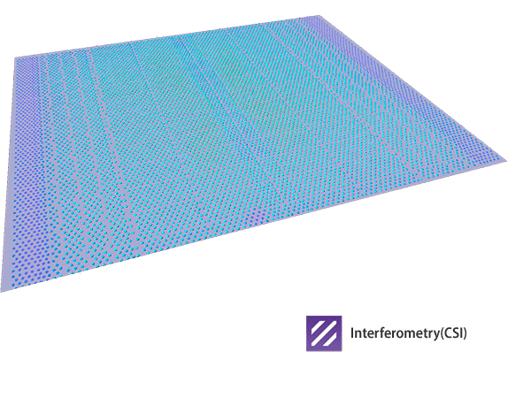
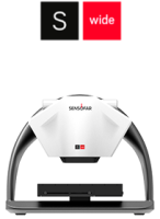
This corresponds to the cover of an electrical communication device used in a 5G base station. From an acquisition point of view, the S wide perfectly suits the demand for speed; the 145x121mm measurement was imaged in 2.5 minutes. As for the analysis, having the option of a circular profile has been critical to solve the application. From that circular profile, we applied the criteria to process profiles, the ISO 4287 and extracted the waviness values.


