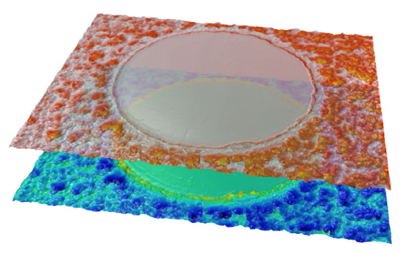
Using optical areal measurement methods to assess the surface shape and texture on aluminium anodized surfaces
2013年にアメリカ合衆国向けの応用エンジニアとしてSensofar Metrologyに入社。2015年にSensofar Medicalに異動し、セールスマネージャーに就任。現在、医療機器業界におけるSensofarの革新的なステント検査技術の導入を指揮している。
Using optical areal measurement methods to assess the surface shape and texture on aluminium anodized surfaces publication
A. Arasanz 1, N. Schwarz 1, A. Matilla 1, J. Mariné 1, R. Artigas 2, C. Cadevall
1 Sensofar-Tech, S.L. (Spain)
2 Universitat Politècnica de Catalunya (UPC) Rambla Sant Nebridi, 10, E-08222 Terrassa, Spain
Aluminum Andoizers Council Conference & Exposition
September 16-18 2014, Pittsburg, Pennsylvania, USA
Project: Confocal Microscopy
Abstract
Any optical system used for the surface finish measurement of an anodized part needs to recover the signal from the air-‐ano layer, which is very weak in comparison to the signal on the ano-‐aluminum layer. Confocal based optical systems work very well for this purpose, but they have the drawback of having to use high numerical aperture objectives, only possible with high magnification, and thus the need to use stitching to recover millimeter scale. This makes the measurement a slow task and not suitable for production environments. On the other hand, Coherence Scanning Interferometry (CSI) based systems can evaluate larger areas while keeping good signal separation between both interfaces. Some optical measurement systems can combine both, Confocal and CSI, for the evaluation of surface texture in the aluminum and the oxide layer at the same time. This makes it possible to characterize defects in 3D prior to the anodization process as well as assessing the quality of the final product.
1. Introduction
Aluminum is being most and most popular in consumer electronics as a high quality product. This market introduces new challenges to traditional measuring methods of surface finish and layer thickness of anodized parts, such as the machining of small parts with complex shapes, ultra-high quality decorative finish, cosmetic features on aluminum substrate or the anodic layer, specific surface texturing, and deep color dying on thick anodic layers. All these processes have typically sub millimeter features, which need to be measured with high lateral resolution.
When the focus is to assess the coating thickness, the most common measuring method uses the eddy current effect. The coating thickness is measured as the impedance change between the conductive substrate and the measuring coil, which is equal to the anodic layer. Despite the benefit of simplicity of eddy current systems, the method is influenced by curvature in the part, thickness of the substrate, surface roughness, and contact force, giving non-accurate readings. Optical non-contact methods rely on fiber based spectrometers and spectroscopic reflectometry. These instruments illuminate the measuring area with a spot of light coming from a white light source. The reflected light is recovered by a fiber optic and directed onto a spectrometer, which splits the white light to its wavelength components. Each wavelength is the combination of the light reflected from the aluminum substrate and the anodic layer, being the result a constructive or destructive interference depending mainly on the coating thickness. Analyzing the interference spectrum and comparing to a theoretical model these instruments can recover layer thickness with very high resolution. Both methods are non-destructive and can be handheld units, but they share two limitations when the focus is to asses surface finish: they are assessing the layer thickness of a relatively large area of a single spot, and they are measuring anodic thickness but not surface topography. However spectroscopic reflectometry can be conducted through a microscope, achieving higher lateral resolution. Therefore by scanning the spot on the surface a three-dimensional map of the layer thickness can be recovered. Surface texture measurements in the sub-millimeter lateral scale are achieved with Contact Stylus profilers, Atomic Force microscopes, and Optical measuring instruments. Contact Stylus and Atomic Force profilers can sense the most exterior layer (the ano-air interface), but not the aluminum substrate or the coating thickness. Optical measuring instruments can be based on single point measurement or on area scanning. The latter ones measure many points at the same time by the use of an imaging device, like a CCD camera, and thus achieving the final three-dimensional result much faster than in-plane scanning systems. The two most common technologies of area scan optical measuring instruments are Confocal and Coherence Scanning Interferometry (CSI), formally known as White Light Interferometry. Next section describes how these technologies perform on anodized aluminum samples.
2. Confocal and Interferometry on anodized aluminium
2. Confocal and Interferometry
on anodized aluminium
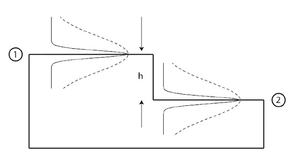
The resulting image from a Confocal microscope is an image that supresses the light falling outside from the depth of focus of the objective, while it preserves all the light that is in the depth of focus. This image is called an optical section. Three-‐dimensional measurements on a Confocal microscope are achieved by scanning the surface through the depth of focus of the microscope and recording a series of optical sections. The height location for each pixel is calculated as the height corresponding to the optical section within all sections where this pixel achieves its highest signal. The width of the optical section is close to the depth of focus, which is narrower the higher the Numerical Aperture (NA) of the objective, and the shorter the wavelength of the light source. Confocal microscopes can achieve nanometer level height resolution on its best with the use of the highest numerical aperture dry objectives, typically 0.95 corresponding to magnifications of 50X or higher. Figure 1 shows a step like surface where the top is located at point 1 while the bottom is located at point 2. A confocal microscope will generate a signal, called axial response, similar to a Gaussian where its maximum is located at the surface and the width depends on the Numerical Aperture as shown in Figure 1.
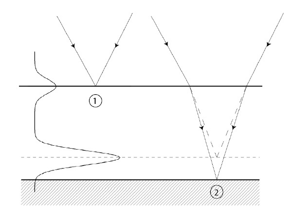
A confocal microscope can also be used to measure the surface of a material that has been coated with a transparent film. In this situation, two peaks are appearing on the axial response at each point, one corresponding to the coating-air interface, and a second one corresponding to the coating-substrate interface. The location of the first peak corresponds to the location of the surface, while the location of the second peak is no longer on its correct position due to focusing effects through transparent media [flagello]. Layer thickness can be recovered with the appropriate model that describes the focusing effect and good knowledge of the light properties, Numerical Aperture of the objective and refraction index of the coating layer [Cadevall]. Figure 2 shows substrate focus shift (point 2) when focusing through a transparent media.
With the appropriate algorithm, a Confocal profiler can measure three topographies in anodized aluminum: the ano-air layer topography, the ano-aluminum topography, and the difference between both, that equals to the thickness map with the corresponding correction model. This technology is limited by two major constraints. The first one is that the thinner the layer, the narrower needs to be the axial response to avoid overlapping of the signals from both interfaces; the second limit is that the focus shift of the ano-aluminum interfaces is closer to the ano-air. These two limits can be minimized having the axial response as narrow as possible, which is achieved with the highest possible Numerical Aperture, 0.95 for dry objectives. The axial response width for an objective with 0.95 NA and 0.55 µm light wavelength is about 0.75 µm, limiting the minimum resolvable layer thickness to 1.5 µm. Additionally, such high Numerical Aperture is only possible with high magnification, from 50X and above, with a field of view of few hundreds of square microns, and thus imposing the need to do field stitching in order to assess large surface areas.
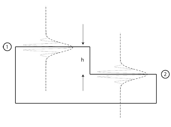
In contrast to a Confocal microscope, a Coherence Scanning Interference (CSI) microscope achieves the three dimensional measurement of a surface by locating the best contrast position of an interference signal acquired though the depth of focus of an interferential objective. Figure 3 shows the interference signal on a step surface (solid lines) and its signal envelope (dashed lines). The width of the interference signal envelope is related to the coherence length of the light source. The shorter the coherence length, the narrower the signal envelope. The Numerical Aperture of the objective is also playing a small role on the envelope width, being narrower with higher NA values. The narrowest signals are given with the shortest possible coherence length light source, that for practical purposes is a white light source as continuous as possible. Incandescent light bulbs and white LEDs are typically used.
For anodic layer thickness and topography measurement, two effects arise from an interferometer. The first is that the interference location for the aluminium substrate appears deeper than the real location of the aluminium. This is due to an optical path difference between the air and the anodic layer. Figure 4 shows this effect, causing the interference signal to appear about two times deepper than the aluminium substrate. The second effect, as it happens with a confocal microscope, is that the aluminium substrate image is shifted closer to the ano-air layer. The separation of the interference signals between the ano‐air layer and the ano‐aluminum layer is a benefit, making easier to measure thinner layers in comparison to Confocal microscopes. But on the other hand, the thicker the layer, the more shift between the substrate image and the interference signal, making the interference contrast to fall. To minimize this problem, a lower Numerical Aperture objective is preferable, causing the shift to be not so critical and making possible to measure thicker coatings. In practice, the minimum resolvable thickness layer with an interferential microscope is about 1 micron, while the thickest is about 30 microns.
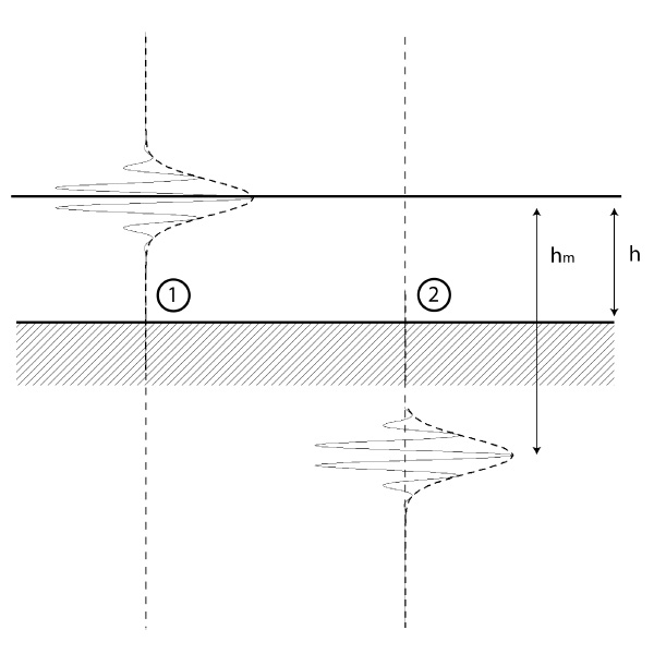
The benefit of using an interference microscope for the measurement of anodized aluminium topography and the anodic layer thickness, is that the measurement can be achieved within the field of view of a low magnification objective without sacrificing height resolution and without the need to do field stitching in order to assess large surface areas.
3. Results
In order to check technology performance, we selected two parts of a laptop computer, on which aluminium was used as main body and an anodic layer was grown on it. One part of the main body had a mirror-‐like finish, and a second part had laser engraved features on the aluminium substrate.
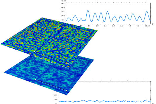
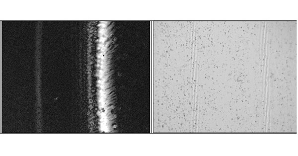
Figure 5 shows the confocal and interferential images taken with a 100X 0.95NA objective for the confocal image, and a 20XDI 0.45NA objective for the interferential one, both with white light. The images were taken on the smoothed aluminium part with particles and scratches. Signals coming from the air-‐ano layer are on the left of the image and the ano-‐aluminum layer on the right. Note that in the case of the confocal signals, the ano-‐air signal is much weaker, while on the ano-‐aluminum layer is stronger due to its higher surface reflection. Note also that the reflection on the substrate exhibits secondary reflections that will disturb the ability to split correctly the two signals on those pixels where the signal from the top layer is very weak. For the interferential signal, you can note that the fringe contrast on the ano-‐air layer (left signal) has much better contrast than the fringes on the ano-‐aluminum interface, due to defocus of the substrate as explained in section 2.
The resulting topographies of the images in figure 5 are shown on figures 6 and 7. With Confocal technology we had the ability to show the smoothness of the anodic layer and the aluminium substrate with the embedded particles. Lateral field of the measurement was 150 x 125 microns and the layer thickness was 10 micron. Particles dimension are in average between 5 and 10 microns length and between 1 and 2 micron height. The measurements were obtained using S-‐neox commercial system from the company Sensofar Tech SL. The software requires the use of the refraction index of the anodic layer to recover the correct topography of the aluminium substrate and evaluate the layer thickness map.
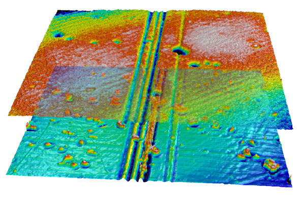
Figure 7 shows the ano-air interface and the ano-aluminum interface topographies of a similar region of figure 6, but using CSI with a 20X DI objective and 20 micron scanning range. Overall measuring time was less than 20 seconds including scanning and data processing to split the two signals and evaluating the topographies on both interfaces. The surface roughness on the ano-‐air interface was 20.8 nm (Sq) with a peak to valley of 138 nm, while the roughness on the polished aluminum was 44.6 nm (Sq) and a peak to valley of 376 nm. Layer thickness was 9.55 micron in average with a mean deviation of 0,057 micron.
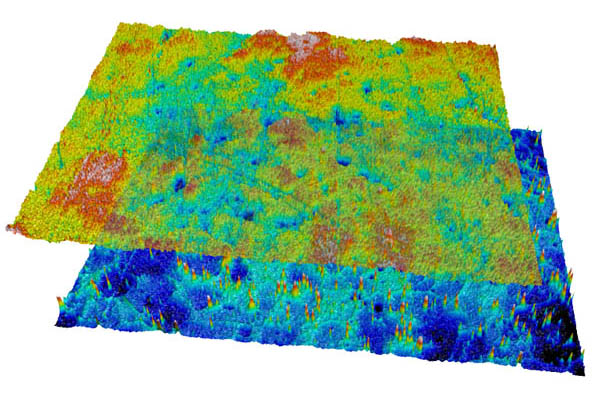
A second feature on the computer body was selected to demonstrate the ability of optical three-dimensional methods to measure small surface features on aluminum parts. The selected region was a laser engraved part containing the serial number of the computer prior to the anodizing process. Figure 8 shows the result of the ano-air and ano-aluminum interface topographies measured with CSI using the same settings as for the results shown in figure 7.
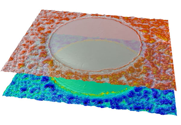
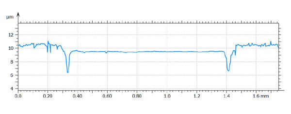
Figure 9 shows the central profile corresponding to the thickness of the two topographies from figure 8. Notice that the anodic layer has grown faster on the rougher part than on the smoother region where the laser engraving was done.
4. Conclusions
Confocal and Coherence Scanning Interferometry (CSI) have shown to be good technologies to measure the three dimensional surface texture and shape of aluminium anodized parts with high lateral resolution. Confocal has the benefit of being able to use high magnification in order to provide measurements of micron-size features, while CSI keeps good signal separation for lower magnifications enabling the characterization of surface texture on the millimetre lateral scale.
References
Roger Artigas, Agustí Pintó, and Ferran Laguarta, “Three-dimensional micromeasurements on smooth and rough surfaces with a new confocal optical profiler”, in the Optical Measurement systems for industrial inspection, Vol. 3824, pp 93-‐103, Munich (1999).
Cristina Cadevall, Roger Artigas, and Ferran Laguarta. “Development of confocal-based techniques for shape measurements on structured surfaces containing dissimilar materials”. Spie Vol 5144, 206-‐217 (2003).
D. G. Flagello, T. Milster, and A. E. Rosenbluth. “Theory of high NA imaging in homogeneous thin films”. J. Opt. Soc. Am. Vol 13, N-‐1 (1996).


