为何使用三合一技术?
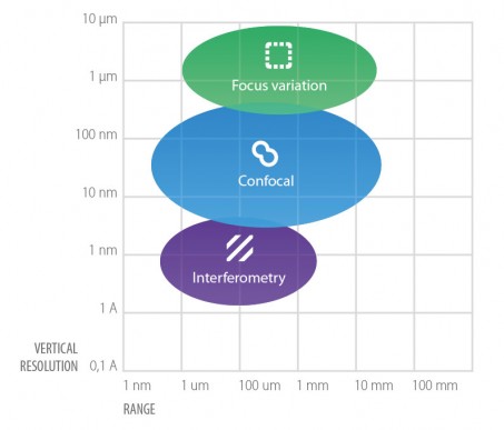
S neox 秉持了最初的设计目标,作为一台具有高性能的3D 光学轮廓仪,超越了现有的一切光学轮廓仪。S neox 结合了三大技术——共聚焦(最适用于高斜率表面)、干涉(有最高的垂直分辨率)和多焦面叠加(在短短几秒内测量形貌特征),将三大技术集于一体,且不用任何运动部件。

共聚焦
共聚焦轮廓仪能测量从较光滑到非常粗糙的表面,空间采样精细至0.10 μm,是关键尺寸测量的理想选择。高数值孔径(0.95)和高放大倍率(150X)的物镜可用于测量局部斜率超过70° 的光滑表面以及斜率高达86° 的粗糙表面。我们的专利共聚焦算法能实现纳米级的垂直方向重复性。

多焦面叠加
多焦面叠加是设计用于测量大面积粗糙表面的光学技术。Sensofar 采用该方法专门用于补足放大倍率较低的共聚焦测量。该技术的亮点包括高斜率表面(高达86°)、最快的测量速度(mm/s)和较大的垂直扫描范围。这些特性的结合十分适用于工具加工的应用。


分光光度计
分光光度计能快速、精确、无损地测量薄膜,且无需制备样本。采集的干涉光谱会在软件中进行模拟,优化膜层厚度和折射率,直至实现最佳匹配。该技术十分适用于单层箔、膜和基板上的多层薄膜(1 到10层)。可在一秒内以0.1 nm 的厚度分辨率和高达5 μm 的横向分辨率测量从10 nm 到20 μm 的透明薄膜厚度。
我们是如何做到的?
关键在于microdisplay!Microdisplay结合高分辨率的电动平台和可更换的物镜构成了一套灵活的光学系统。在microdisplay产生变化的狭缝,结合明场物镜,构成了共聚焦显微镜的基本要素。把狭缝全部打开变成平面,系统便能实现多焦面叠加。如将明场物镜更换为干涉物镜,系统便能实现干涉。
What does 3D Surface Metrology measure?
Very generally, both natural and manufactured surfaces comprise a primary shape or form (topography), with varying degrees of structure, waviness and roughness (2D/3D). All of these surface features will contain both intentional and unintentional (controlled/uncontrolled) contributions.
The relative significance of these contributions is determined by the application (noting that uncontrolled contributions are not necessarily undesirable). The goal of a measurement is to evaluate – qualify and quantify – the differing contributions, either in support of a fundamental scientific research finding, or with regard to a target industrial application.
Depending on the field or application, the structure, waviness and roughness contributions might be categorized as finish, haptic, texture, defects, marks, micro-wear and much more. Alternatively, the user may be looking to determine critical dimensions, step-height, peak-to-valley, volume or slope, or even map coating thickness and other surface characteristics.
If the goal is to determine areal (3D) surface texture, the results can be also be rigorously tied to the appropriate parameters as defined by the increasingly prevalent ISO 25178 standard. In industrial (surface) manufacturing, the adoption of best practices tied to widely accepted standards can make manufacturing more efficient, reproducible and traceable.
Typical applications sectors include general scientific and materials research, optoelectronics, data storage, automotive, medical technology, energy, and optics & optoelectronics. Specific applications include additive manufacturing, automotive and consumer electronics, ballistics, CMP pad monitoring, micropaleontology, nano-technology, micromanufacturing, optics, surface inspection, surface functionality and passivation.
The sheer breadth of 3D surface and 2D profile metrology tasks across so many scientific and industrial applications points directly to the outright practicality of Sensofar Metrology’s ‘3-in-1’ approach.


